

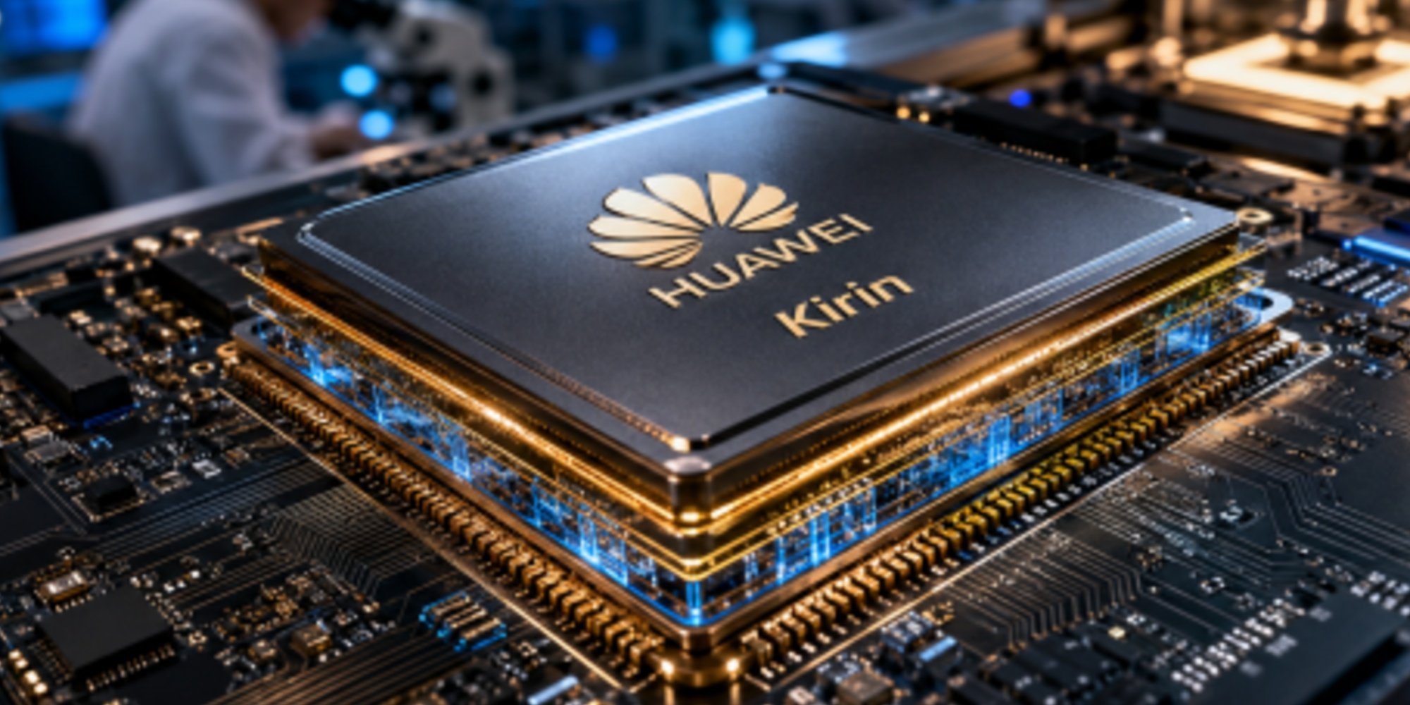
On May 25, 2026, He Tingbo, president of Huawei's semiconductor department and board member of the group, presented the Tau (τ) scaling law and the LogicFolding architecture at the IEEE ISCAS conference in Shanghai. These are intended to bypass the reliance on ASML's extreme ultraviolet (EUV) lithography machines. The publisher claims a transistor density 55% superior to conventional planar designs, a figure not independently verified, aiming for 2031 to achieve a density equivalent to a 1.4-nanometer process through 3D architectural design, not actual etching at this fineness. The first Kirin chips featuring LogicFolding are expected in fall 2026. In Hong Kong, the stock of Chinese foundry SMIC jumped 7.6% on the day of the announcement, according to CNBC.
A Temporal Scaling Law to Succeed Moore
Huawei's theoretical proposal involves replacing Moore's law's geometric scaling with a temporal scaling, where the optimization variable is the signal propagation delay measured across the entire computing stack. While the industry's historical trajectory has relied on reducing the etching pitch—a purely physical metric—the quantity τ proposed by Huawei targets the time it takes for a signal to traverse a logical chain, whether organized flat or in relief. The publisher claims to have designed and mass-produced 381 chips based on this principle over the past six years, a claim that remains self-declared and without external academic validation as of May 25, 2026. According to Huawei, as reported by CNBC on May 25, 2026, the roadmap projects extending LogicFolding to Ascend chips, presented as domestic substitutes for Nvidia's training GPUs banned from export to China, by 2030. The context of this timeline is not indifferent: according to a report published by the Information Technology and Innovation Foundation in October 2025, U.S. export controls have paradoxically stimulated Huawei's internal capabilities, forcing the group to independently rebuild competencies that TSMC provided until 2020.
Moore optimizes the etching pitch. The Tau law optimizes signal propagation delay across the entire stack.
Huawei does not propose a lithographic advance—it proposes to change the optimization variable itself.
LogicFolding: 3D Against EUV, and Its Shades
The LogicFolding architecture involves stacking the active layers of a logic circuit in three dimensions, shortening electrical paths and maximizing transistor density by ground projection without relying on ASML's EUV lithography machines. The gain logic does not concern etching fineness, which remains limited by the equipment accessible to Huawei and foundry SMIC, but on the vertical organization of the substrate: additional density is achieved by multiplying transistor levels above the same silicon footprint, at unchanged etching pitch. The claimed equivalence for 2031 with a 1.4 nm process is thus an effect of counting by ground projection, not the physical ability to trace patterns at this resolution. In an interview with CNBC on May 25, 2026, Paul Triolo, technology lead for Asia and the Americas at DGA Group, nuances the scope of the announcement: according to him, a stacked or folded design can produce effective density gains, but it does not mean Huawei has solved the full process, yield, power, thermal, and device-performance problems associated with true 1.4 nm-class manufacturing. No public data on yield, consumption, or thermal performance accompanies the announcement at this stage.
1.4 nm: An Equivalent Density, Not Etching Fineness
Huawei's 2031 goal targets an architectural density equivalent to the 1.4 nm node, achieved by vertical stacking (LogicFolding)—not actual 1.4 nm lithography. Paul Triolo (DGA Group, CNBC) states the limitation: “a stacked/folded design can produce effective density gains, but it does not mean Huawei has solved the full process, yield, power, thermal, and device-performance problems associated with true 1.4 nm-class manufacturing.” No data on yield, consumption, or thermal performance has been published at this stage.
A 3D Architecture That Isn't Uniquely Huawei's
The 3D stacking of active layers is not an innovation unique to the Shenzhen group. Several Western and Korean foundries and designers—Samsung, TSMC, and Intel in particular—have been deploying comparable 3D stacking approaches for several years for commercial competitiveness rather than circumventing export sanctions. The specificity of LogicFolding lies less in the architectural idea than in the context in which it is mobilized: that of a publisher cut off since 2020 from leading Western foundries, deprived of access to ASML's lithography machines. The movement is part of a broader Chinese dynamic of autonomy in the computing chain, with the clearest political signal being the summoning of Nvidia by Beijing in July 2025 regarding H20 chips, reflecting China's desire to extricate itself from a dependence considered a security risk.
He Tingbo, the Tutelary Figure of HiSilicon
The institutional authority of the dossier bearer conditions the sectoral reading of the announcement. According to the official profile published by Huawei, He Tingbo simultaneously holds the positions of board director, president of the Scientist Committee, director of the ITMT (Information Technology Management Team), and president of the semiconductor department (HiSilicon). This concentration of mandates—governance, scientific committee, operational execution—places her at the intersection of the group's technical and political arbitrations. HiSilicon, the design subsidiary of the Huawei group, assured its runs at TSMC until 2020. The Taiwanese foundry interrupted this relationship following the extraterritorial extension of US sanctions on semiconductor exports, through Huawei's listing on the Entity List (entities subject to export restrictions from the United States) and the extension of the Foreign Direct Product Rule (extraterritorial rule prohibiting third-party foundries using US technology from delivering to Huawei), forcing the group to rebuild its design chain with SMIC for production and invest massively in its architectural design. The choice of the IEEE ISCAS platform in Shanghai to present the τ law places this reconstruction in the international academic register rather than just corporate communication.

Our articles will then appear first in Google Top Stories.