TLDR : Sony announces the launch of the IMX479 SPAD sensor for automotive LiDAR, enhancing precision and speed for ADAS and autonomous driving systems.
Table of contents
Sony Semiconductor Solutions Corporation (SSS) announces the upcoming launch of the stacked SPAD depth sensor IMX479, designed to enhance the precision and speed of automotive LiDAR systems. Utilizing the direct Time of Flight (dToF) method, this sensor offers unprecedented performance, essential for ADAS (advanced driver-assistance systems) and AD (autonomous driving) technologies.
A differentiating technological positioning
The IMX479 sensor is based on a stacked SPAD (Single-Photon Avalanche Diode) architecture, combining a back-illuminated dToF pixel array with embedded measurement logic on a single chip, thanks to copper-to-copper (Cu-Cu) connections. The elementary detection unit consists of 3×3 pixel blocks, optimized for linear scanning. This configuration allows for a record speed of 20 frames per second — the highest at this resolution level (520 dToF pixels) — while maintaining a reduced pixel size of 10 µm. It thus reconciles processing speed and resolution finesse, two qualities rarely combined in automotive LiDAR systems.
Precise detection, even at long distances
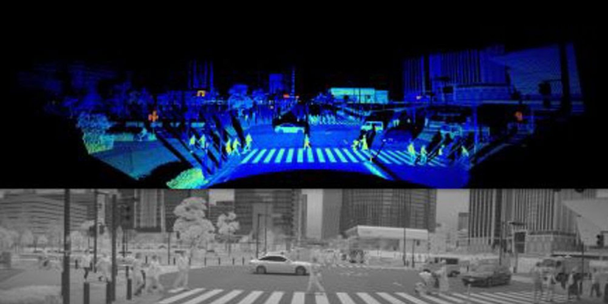
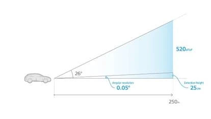
Among the announced features, some particularly stand out: a vertical angular resolution of 0.05 degrees (an improvement of 2.7 times compared to previous generations) and the ability to detect objects 25 cm high, like a tire on the road at 250 m, or even up to 300 m thanks to photon detection efficiency of 37% at 940 nm. This level of performance opens new possibilities for ADAS systems and embedded perception algorithms, enabling better 3D modeling of the road environment, even in extreme lighting conditions.
To promote its adoption, SSS has developed a mechanical scanning LiDAR equipped with the sensor, allowing automotive manufacturers and partners to evaluate its efficiency before integration.
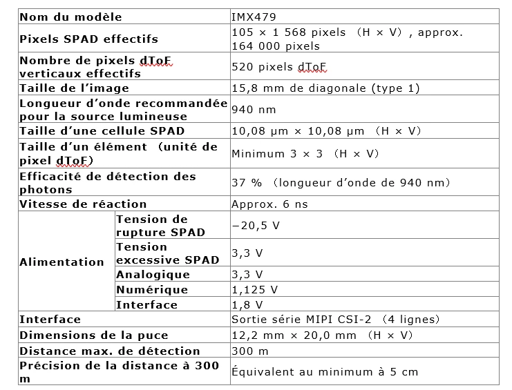
Technical sheet
Enhanced vertical integration logic
Sony leverages its historical expertise in CMOS sensors while pursuing a vertical integration strategy. The use of advanced packaging technologies, such as Cu-Cu interconnections and stacked architecture, aligns with a desire for complete control of the technological chain — from photonics to system architecture. This approach not only maximizes performance but also reduces bulk and costs in the long term.