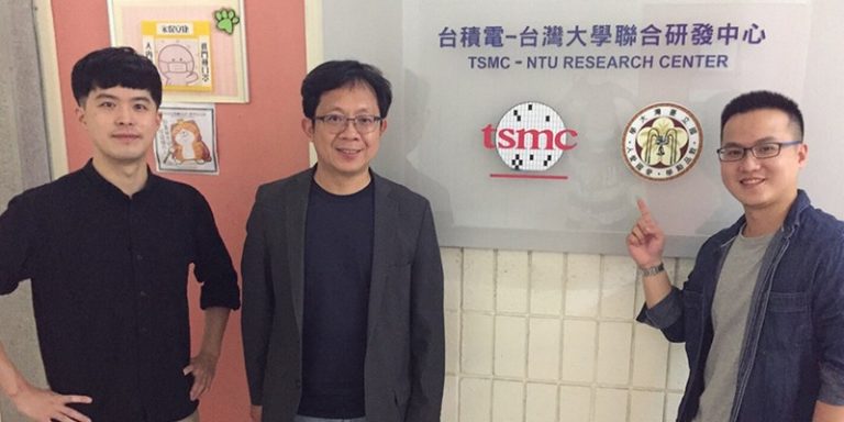
Earlier this month, IBM announced its new 2-nanometer chipaimed at high performance. In a close collaboration between the Massachusetts Institute of Technology (MIT), the National Taiwan University (NTU) and the Taiwan Semiconductor Manufacturing Company (TSMC), several researchers have succeeded in developing electronic circuits from two-dimensional materials. This discovery would bring us one step closer to the realization of 1-nanometer etchings.
MIT, NTU and TSMC research to push the limits of etching
Currently, chips used in electronic devices range from 5 to 16 nanometers. Despite the announcement of IBM’s new 2-nanometer etch technology, the chip is not yet in use or even commercially available. The move from 16 to 5 nanometers was made possible by the development of new generations of manufacturing processes that allowed the addition of more transistors on a smaller surface, increasing the performance of the chips tenfold.
In a study jointly conducted since 2019 by MIT, NTU and TSMC, researchers have made a discovery around new semiconductor design that could lead to pushing the etch fineness to 1 nanometer. The findings were published in a paper led by Pin-Chun Shen, a researcher in MIT’s Department of Electrical Engineering and Computer Science.
A new technique for a 1-nanometer chip
The research team focused on the transistors that make up electronic chips. Typically, chips are built using layers of silicon arranged in three dimensions. However, this process is gradually reaching its physical limits and it is difficult to imagine that a chip could be etched to less than 2 nanometers using this technique. Instead of using this manufacturing method, researchers have turned to two-dimensional materials. Graphene is one, probably the best known, but the one that has been exploited is bismuth.
They have tried to design transistors in two dimensions, instead of three, using a very thin “foil”, an electrode made of semi-metallic bismuth and an ionized helium lithography machine. The researchers claim that this process retains the same performance and behaviour as a conventional silicon transistor. They say that single-layer (or two-dimensional) transistors are just as efficient as three-dimensional ones, which could lead to a reduction in etch size.
Nevertheless, Cong Su of MIT’s Department of Nuclear Science and Engineering did state in his remarks that no 1-nanometer chips have been produced:
“Many publications and media coverage claim that this work is a breakthrough for 1nm etching. While we agree that this solves a major problem for the creation of single-layer transistors, we have not fabricated for this publication any device […] that meets the 1nm standard.”
While this study is the first step towards one-nanometer etching, there is still a long way to go to get there.
Translated from Vers une gravure en 1 nanomètre : le défi des chercheurs du MIT, du NTU et de TSMC


