

After presenting its next humanoid robot at Tesla AI Day, Elon Musk’s firm announced the future design of Tesla Dojo D1. This chip dedicated to the training of artificial intelligence should allow Tesla vehicles to ensure a semi-autonomous driving thanks to the supercomputer features it has. Despite the fact that its design is relatively expensive, for the company, this chip represents a major stake in the competition against Infineon, Renesas and NXP.
A new Tesla Dojo D1 chip to boost Autopilot and semi-autonomous driving
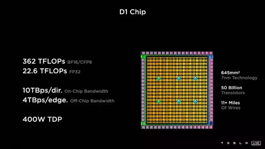
During the Tesla AI Day that took place on August 19, 2021, the Tesla Dojo D1 chip was unveiled. Presented by the company as having “the computing power of a GPU with the flexibility of a CPU”, it will be dedicated to AI training. The chip was developed entirely in-house and is based on an ASIC platform with 50 billion transistors on a 645mm2 die, all etched at TSMC in 7nm.
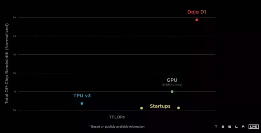
The chip will centralize and process all the information provided by the network of cameras and semiconductors to optimize the operation of Autopilot and achieve true 100% autonomous driving, which is the brand’s goal. According to Tesla, the D1 chip develops double the bandwidth of current chips used in networks.
By designing such a high-performance chip, the company hopes to maintain low latency and maximum bandwidth.
Tesla Dojo D1’s strength in numbers
The compiler specifically created to train AI and boost Tesla’s Autopilot will offer 362 TFLOPs of processing power in FP16/CFP8 (Configurable FP8) precision and 22.6 TFLOPS in FP32 precision, which is basically more than the 312 TFLOPS in FP16 of the Nvidia A100 accelerator (under Ampere).
Tesla Dojo D1 consists of 354 functional units and the company will not hesitate to link the chips together to compose a set of 500,000 functional units that will be leveraged for its AI training needs. More than 17 kilometers of cabling will be used to connect all these components. Note that for its operation, the chip must require a power of 400W.
Testa’s future ambitions with the Training Tiles
With the help of this chip, Tesla has created Training Tiles. This structure consists of 25 Dojo D1s connected together in a square with I/O interfaces at the edge. By keeping this arrangement, a bandwidth of 9 TB/s per side is guaranteed, i.e. 36 TB/s in total, and the fabric can develop 9 PFLOPs of processing power.
The first Training Tiles was tested shortly before its presentation at Tesla AI Day. The goal for Elon Musk’s company is to create sets of Training Tiles, linked together to develop a processing power of 100 PFLOPs. Even stronger, in the long term, the firm’s experts want to connect a large number of Training Tiles in order to offer an ExaPod with a processing capacity of 1 EFLOPs/second.
Translated from Retour sur la puce d’entrainement d’intelligence artificielle Tesla Dojo D1 présentée lors du Tesla AI Day


